
Products
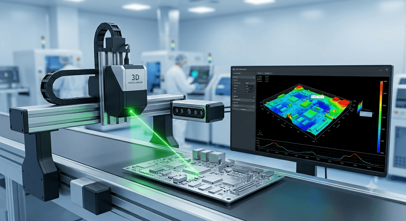
3D Machine Vision Inspection System (Automated Inspection)
The 3D machine vision inspection system uses high-precision 3D shape measurement to accurately detect subtle height and shape defects on semiconductor bumps and surfaces — a fully automated inspection solution.
Key Features
High-precision Shape Measurement
Sub-micron height resolution precisely measures bump coplanarity.
3D Profile Visualization
Visualizes measurement results as 3D profiles for clear defect judgment evidence.
Broad Package Compatibility
Flexibly supports various semiconductor package types including WLP, FC, and BGA.
Automatic Defect Classification
Automatically classifies defect types to support root-cause analysis and yield improvement.
Applications
- Semiconductor bump coplanarity inspection
- Package surface shape inspection
- Bonding wire loop height measurement
- PCB solder paste shape inspection
Image Gallery
Considering new inspection equipment?
Review specifications and use cases, then request a tailored quote.